Design Guideline -
The Internal PI Compensator of an off-line Flyback Converter for USB Power Delivery Applications
Abstract
In order to reduce the external components of an off-line flyback converter for USB Power Delivery applications, an Internal Proportional and Integral Compensator (IPIC) is proposed and integrated into Richtek’s Secondary-Side controller (SSC) to provide a regulated output with Constant Voltage (CV) and Constant Current (CC). With the additional phase-boost circuit, the Type-II compensator is resulted to stabilize the flyback converter. This application note provides a comprehensive design guideline to determine specific coefficients of the IPIC and the phase-boost circuit so as to optimize the transient response of a flyback converter for USB PD applications.
1.
Architecture
of the Feedback Circuit of the Flyback Converter
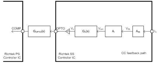
Figure 1 shows the architecture of the flyback converter’s feedback of the Primary-Side (PS) and the Secondary-Side (SS) in the Richtek's USB PD Controller IC. Both output voltage, Vo, and output current, Io, of the converter are sensed to the SSC. The internal output voltage feedback signal, Vvfb, is obtained from the voltage divider with a ratio determined by RF1/(RF1+RF2). The feedback voltage, Vvfb, is then compared with the set reference voltage, VVREF, and the voltage error signal, Vverr is obtained. Meanwhile the internal output current feedback signal, Vifb, is obtained from the current sensing resistor, RCS, and fed to the Current Sense Amplifier (CSA). The current error signal, Vierr is then obtained by comparing the Vifb with the set reference current, VIREF.
Two diodes are used for the Error Selector to select the dominated control signal, i.e., the higher voltage from Vverr or Vierr. The higher one is designated as the dominated error signal, Verr. If Vverr is selected, the Constant-Voltage (CV) loop of the converter will be regulated. On the other hand, if Vierr is dominated, the Constant-Current (CC) loop will be regulated.
After the error signal, Verr, is compensated by the IPIC, the output of the IPIC, Vc, is buffered and sent out via the OPTO pin to drive the external optocoupler’s opto-diode. Through an isolated optocoupler, the compensated signal will be sent to the COMP pin on the Richtek Primary-Side (PS) Controller IC in order to adjust the PWM duty cycle and control the output power of the primary switch.
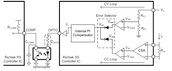
Figure 1. Architecture of the feedback circuit
2.
The Transfer
Function of Internal PI Compensator, Gc(s)
Figure 2(a) shows the block diagram of a typical PI compensator. The output signal, Vc, is processed by the Proportional-Controller (P-Controller) and the Integral-Controller (I-Controller) from the error signal, verr. The PI compensator can be implemented by an Operational Transconductance Amplifier (OTA) consisting of the transconductance, gm, a resistor, Rc, and a capacitor, Cc, as shown in Figure 2(b). As depicted in Fig. 2(b) assuming the OTA has the high output impedance, the transfer function of the IPIC is obtained as follows.
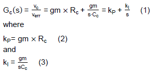
According to Eqs. (2) and (3), one can adjust the control loop’s response by tuning the IPIC’s parameters, gm, Rc and Cc.
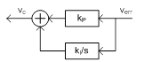
(a). Signal block diagram of the PI compensator
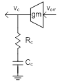
(b). Circuit of the PI Compensator
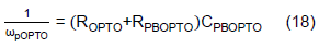
Figure 2. Internal PI Compensator
In some applications, it is more practical to design the IPIC’s parameters in the frequency domain, for that one can rearrange Eq. (1) as the following equation,
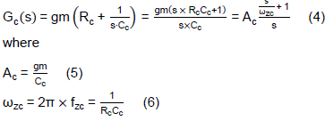
Eq. (4) shows the transfer function of IPIC, Gc(s), has a pole at zero frequency and a zero at fzc. Therefore, the output phase of Gc(s) will be -90° at low frequency and turn to 0° when the input signal’s frequency is higher than the IPIC’s fzc.
The gain of the IPIC can be further derived as the following equation.
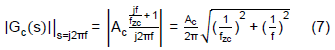
If 1Hz sine wave is injected to the IPIC and fzc is larger than 10Hz, Eq. (7) can be approximated to the following equation.

If the input signal’s frequency is higher than fzc, Eq. (7) can be simplified to
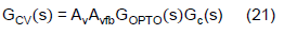
With given gm, Rc and Cc, the fzc, Ac@1Hz and Ac@HF are known. Thus, the frequency response of the IPIC can be determined by the Bode diagram as shown in Figure 3.
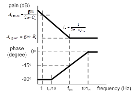
Figure 3. Typical frequency response of the IPIC
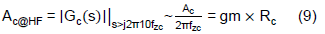
Take an example of the designed IPIC with gm = 20µA/V, Rc = 10kΩ and Cc = 33nF. The correspondent fzc, Ac@1Hz and Ac@HF can be calculated according to Eqs. (6), (8) and (9), respectively.
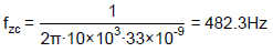


Figure 4 shows the calculated frequency response analysis results.
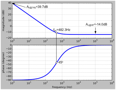
Figure 4. Frequency response of the designed IPIC with gm = 20µA/V, Rc = 10kΩ and Cc = 33nF
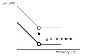
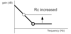
According to Eq. (4) and above analysis, the behavior of the IPIC’s frequency response can be adjusted by the coefficients, gm, Cc and Rc illustrated in Figure 5. Furthermore by using Eqs. (8) and (9), the IPIC’s gain, Ac, can be approximate by Ac@1Hz at low frequency and Ac@HF at high frequency, respectively. The Ac@1Hz is proportional to gm and the inverse of Cc, while the Ac@HF is proportional to gm and Rc. Hence, if gm is increased, both the gains Ac@1Hz and Ac@HF of the IPIC’s frequency response at low and high frequency are increased as illustrated in Figure 5(a). However, as Cc is increased, the IPIC’s gain at low frequency, Ac@1Hz, is decreased and the zero frequency, fzc, is moved to the lower frequency as illustrated in Figure 5(b). If Rc is increased, fzc, is moved to the lower frequency while Ac@HF is increased.
(a)
(b)
(c)
Figure 5. Behavior of the frequency response IPIC according to the change of (a) gm, (b) Cc and (c) Rc
3.
The Transfer
Function from OPTO to COMP, GOPTO(s)
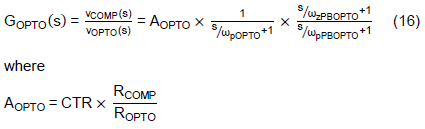
As shown in Figure 1, once the IPIC’s transfer function and the frequency response are defined, the feedback circuit transfer function from the node OPTO at the secondary side of the transformer to the node COMP at the primary side of the transformer can be analyzed, where the OPTO and COMP nodes are isolated by the optocoupler. Figure 6 shows the small-signal model of the signal path from OPTO to COMP, which consists an optocoupler, the optocoupler’s current-clamping impedance, ZOPTO, and the optocoupler’s output low-pass filter formed by RCOMP and CCOMP. Note that the RCOMP is a built-in component in the PS Controller IC, while the CCOMP is the combination of the external capacitor and the parasitic capacitor of the optocoupler. The optocoupler can therefore be modeled as the Current-Control Current Source (CCCS) with the gain specified as the Current-Transfer Ratio (CTR). With that the transfer function of the voltage from the node OPTO to the node COMP is derived as Eq. (10).
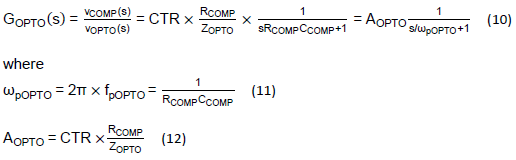
From Eq. 10, GOPTO(s) is a low-pass filter whose pole is located at ωpOPTO if ZOPTO is a resistor. The DC gain of GOPTO(s) can be adjusted by the ratio of RCOMP and ZOPTO.
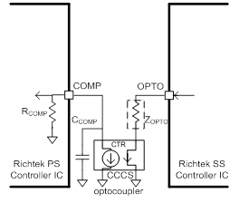
Figure 6. Small-signal model of the optocoupler
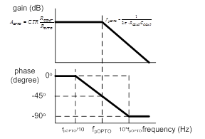
Figure 7. Typical frequency response of GOPTO(s) without the phase-boost circuit
Figure 7 illustrates typical frequency response of GOPTO(S), for example if the parameters are chosen for a ZOPTO = ROPTO = 200Ω, CTR = 0.5, RCOMP = 20kΩ and CCOMP = 10nF, the frequency response is illustrated in Figure 8.
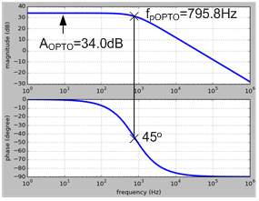
Figure 8. Frequency response of GOPTO(s) with ROPTO = 200Ω, CTR = 0.5, RCOMP = 20kΩ and CCOMP = 10nF
The pole in this example is at 789.8Hz, which is within the loop’s bandwidth. When ωpOPTO is too low and the bandwidth of the loop response will be limited by this pole. As illustrated in Figure 9 the current-clamping impedance, ZOPTO, can be further configured as the so-called phase-boost circuit with the additional RPBOPTO and CPBOPTO in parallel with ROPTO. The admittance of GOPTO(s) can be derived as the following equation which has a zero, ωzPBOPTO, at the low frequency and a pole, ωpPBOPTO, at the high frequency.
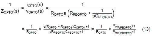


Figure 9. Phase-boost circuit of ZOPTO
From Eq. (14) and (15), ωzPBOPTO has lower frequency than ωpPBOPTO due to the additional ROPTO at the denominator. Since the phase of GOPTO(s) will be increased at ωpPBOPTO, and then decreased at ωpPBOPTO, the phase can be boosted is between the frequency, ωpPBOPTO to ωpPBOPTO. The transfer function GOPTO(s) can be expressed as Eq. (18) when in terms of the phase-boost circuit.
Note that one can use ωzPBOPTO to cancel ωpOPTO and leave the ωpPBOPTO to determine the -3dB frequency of GOPTO(s). Rearange Eq. (14) to get CPBOPTO for a given ωpPBOPTO,

Let ωpOPTO = ωpPBOPTO,
After substitution,

Rearrange

From above equations, the original pole of GOPTO(s), ωpOPTO, is cancelled by the designed ωzPBOPTO and moved to the desired pole, ωpPBOPTO. Thus, the bandwidth limited by the original pole of GOPTO(s) can be extended by the adjustment of the phase-boost circuits’ RPBOPTO and CPBOPTO according to the ratio of the desired and the original pole frequency from Eq. (20).
As illustrated in the example of Figure 8, the pole, fpOPTO, of GOPTO(s) without the phase-boost circuit is located at 795.8Hz, which is too low and will affect the response of the flyback converter. Therefore, we need to add the phase-boost circuit to shift fpOPTO to a 10 times frequency :
ωpPBOPTO = 10 x ωpOPTO
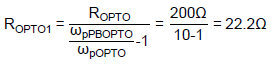
According to Eq. (20),
And Eq. (17),

After obtaining RPBOPTO and CPBOPTO, the phase-boost circuit’s pole and zero from Eq. (14) and (15) are obtained as following frequencies,


To be noted, fzPBOPTO is 795.8Hz, which is the same as fpOPTO. Thus, the original pole is cancelled by the phase-boost circuit. The designed phase-boost circuit’s frequency response is illustrated in Figure 10.
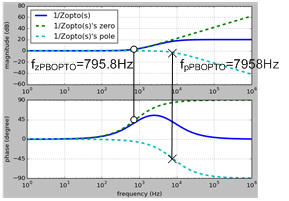
Figure 10. Frequency response of the phase-boost circuit
The following example shows the resulted phase-boost GOPTO(s). As shown in Figure 11, in comparison with GOPTO(s) without phase-boost, the pole is shifted as expected to 10 times original frequency from around 800Hz to around 8KHz
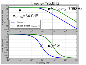
Figure 11. Frequency response of the phase-boost GOPTO(s) compensated with RPBOPTO = 22.2Ω and CPBOPTO = 200nF compared to the original one with ROPTO = 200Ω, CTR = 0.5, RCOMP = 20KΩ and CCOMP = 10nF
4.
The Transfer
Function of Feedback Circuit, GCV(s) and GCC(s)
The small signal model of the feedback circuit as shown in Figure 12 depends on either CV or CC feedback loop illustrated by Figure 12(a) and (b), respectively. The buffer gain from the output of IPIC to the OPTO node is simplified as 1.

(a)
(b)
Figure 12. Small signal transfer function of feedback circuit with (a) CV feedback path, and (b) CC feedback path
The transfer function for CV and CC feedback path are defined as follows.

Assuming the IPIC uses the same coefficients for both the CV and CC feedback path except different gains, once the CV feedback path is designed, the CC feedback path will share the same pole and zero position. By adjusting the CC feedback path’s gain to be less than CV's, the bandwidth of the CC loop will be less than that of the CV loop. Thus, one shall firstly focus on defining the CV feedback path transfer function.
Expand Eq. (21).

If the optocoupler’s pole is cancelled by the phase-boost circuit, Eq. (23) could be further simplified to the following equation.

The transfer function, Eq. (24), reduces to one zero and two poles, so-called Type-II compensator. Figure 13 shows the typical frequency response of the compensated CV feedback path. The designer can determine the frequency respone by well programming the IPIC’s gm, Rc, and Cc and the phase-boost circuits RPBOPTO and CPBOPTO.
Figure 13. Frequency response of the CV feedback path
A typical peak-current mode flyback converter’s power stage has a pole which is determined by its output capacitance and the loading resistance. The zero of the IPIC, ωzcmp, is programmed to compensate the pole of the flyback converter’s power stage. The pole of the phase-boost circuit, ωpPBOPTO, is typically designed at 1 to 10kHz depending on the converter’s bandwidth. The middle gain, ACV, can be designed to have enough phase-margin.
By using parameters as in previous examples, the IPIC’s parameters are gm = 20µA/V, Rc = 10kΩ and Cc = 33nF and the optocoupler is biased with ROPTO = 200Ω which results in CTR = 0.5. The COMP node has RCOMP = 20kΩ and CCOMP = 10nF. The pole created by RCOMP and CCOMP is cancelled via the zero designed by the phase-boost circuit, RPBOPTO = 22.2Ω and CPBOPTO = 900nF.
The green line in Figure 14 shows the frequency response of GCV(s) with the phase-boost circuit. The zero is determined by the IPIC while the 2nd pole is determined by the phase-boost circuit. The cut-off frequency at 0dB of the phase-boost GCV(s) in comparison with the one without phase-boost circuit, is extended.
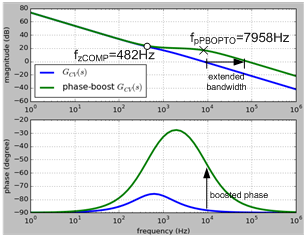
Figure 14. Frequency response of the compensated CV feedback path without (blue line) and with (green line) the phase-boost circuit
5.
Conclusion
The Richtek IPIC is demonstrated with the phase-boost circuit providing a Type-II compensator so as to stabilize a flyback converter. It is guided by the transfer equations, gain, zero and pole of the Type-II compensator can be free determined by the designer to optimize the transient response of different flyback converters under different operating conditions.